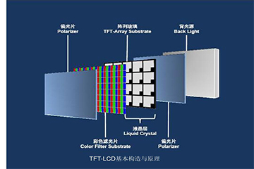

LCD tft display structure
1. The manufacturing process flow of TFT-LCD has the following parts:
①. Form a TFT array on the TFT substrate;
②. Form the color filter pattern and ITO conductive layer on the color filter substrate;
③. Use two substrates to form a liquid crystal cell;
④. Module assembly for installing peripheral circuits and assembling backlights, etc.
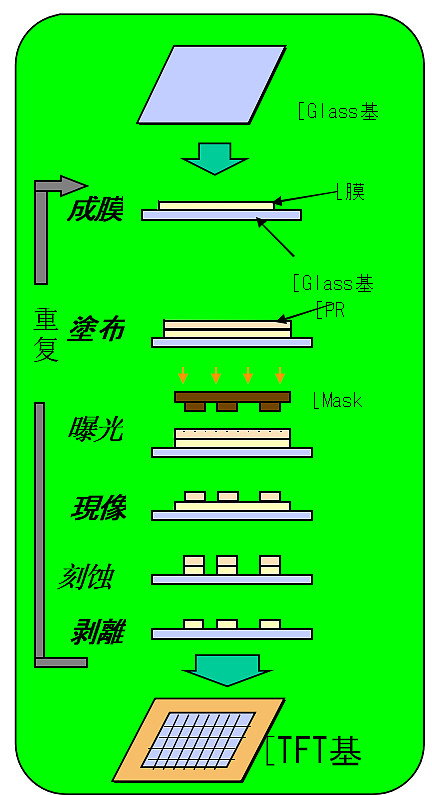
2. Process of forming TFT array on TFT substrate
The types of TFTs that have been industrialized include: amorphous silicon TFT (a-Si TFT), polycrystalline silicon TFT (p-Si TFT), and single crystal silicon TFT (c-Si TFT). Currently a-Si TFT is still used.
The manufacturing process of a-Si TFT is as follows:
①. First, the gate material film is sputtered on the borosilicate glass substrate, and then the gate wiring pattern is formed after mask exposure, development, and dry etching. Generally, a stepper exposure machine is used for mask exposure.
② Use PECVD method for continuous film formation to form SiNx film, non-doped a-Si film, and phosphorus-doped n+a-Si film. Then mask exposure and dry etching are performed to form the a-Si pattern of the TFT part.
③. Use sputtering film forming method to form a transparent electrode (ITO film), and then form a display electrode pattern through mask exposure and wet etching.
④. The contact hole pattern of the gate end insulating film is formed using mask exposure and dry etching.
⑤. Sputter AL, etc. to form a film, use a mask to expose and etch to form the source, drain and signal line patterns of the TFT. A protective insulating film is formed using the PECVD method, and then mask exposure and dry etching are used to etch and shape the insulating film (the protective film is used to protect the gate electrode, signal line electrode ends, and display electrodes).
The TFT array process is the key to the TFT-LCD manufacturing process, and it is also the part that requires a lot of equipment investment. The entire process requires high purification conditions (such as level 10).
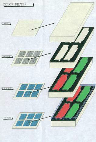
3. The process of forming color filter patterns on color filter (CF) substrates
The methods for forming the colored part of the color filter include dye method, pigment dispersion method, printing method, electrolytic deposition method, and inkjet method. At present, the pigment dispersion method is the main method.
The pigment dispersion method is to disperse fine pigments with uniform particles (average particle size less than 0.1 μm) (three colors of R, G, and B) in a transparent photosensitive resin. Then they are coated, exposed, and developed sequentially to form R.G.B three-color patterns. Photolithography technology is used in manufacturing, and the devices used are mainly coating, exposure, and development devices.
In order to prevent light leakage, a black matrix (BM) is generally added at the junction of the RGB three colors. In the past, sputtering was often used to form a single-layer metal chromium film, but now some use a composite BM film of metal chromium and chromium oxide or a resin-type BM made of resin mixed with carbon.
In addition, it is necessary to make a protective film and form an IT0 electrode on the BM, because the substrate with the color filter is used as the front substrate of the LCD screen and the rear substrate with the TFT together constitutes the liquid crystal cell. Therefore, we must pay attention to the positioning issue so that each unit of the color filter corresponds to each pixel of the TFT substrate.
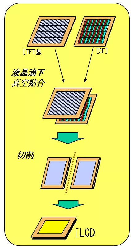
4. Preparation process of liquid crystal box
Polyimide films are coated on the surfaces of the upper and lower substrates respectively and undergo a rubbing process to form an orientation film that can induce molecules to be arranged as required. Then spread the sealant material around the TFT array substrate and spray a gasket on the substrate. At the same time, silver paste is coated on the end of the transparent electrode of the CF substrate. The two substrates are then aligned and bonded to align the CF pattern and the TFT pixel pattern, and then the sealing material is cured through heat treatment. When printing the sealing material, it is necessary to leave an injection port so that the liquid crystal can be filled under vacuum.
In recent years, with the advancement of technology and the continuous increase in substrate size, there have been great improvements in the box manufacturing process. The most representative one is the change in the crystal filling method, from the original post-box filling to ODF. Method, that is, crystal filling and box forming are performed simultaneously. In addition, the padding method no longer uses the traditional spraying method, but is directly produced on the array using photolithography.
5. Module assembly process for peripheral circuits, backlight assembly, etc.
After the liquid crystal box manufacturing process is completed, peripheral drive circuits need to be installed on the panel, and polarizers are affixed to the surfaces of the two substrates. If it is a transmissive LCD, a backlight must also be installed.
Materials and processes are the two main factors that affect product performance. TFT-LCD goes through the above four main processes and a large number of complicated manufacturing processes to form rondelidisplay the products we see.